Ⅰ. Preparation requirements for maintenance platform/tools/equipment
1. Platform requirements:
Static repair workbench (workbench needs to be grounded), anti-static wristband and grounding.
2. Equipment requirements:
(1) Constant temperature soldering iron (350°C - 380°C), pointed soldering iron tip is used to solder small patches such as chip resistors and capacitors;
(2) Hot air gun and BGA rework station are used for chip / BGA disassembly and welding;
(3) Multimeter, with welded steel needles and heat-shrinkable sleeves for easy measurement (Fluke 17B+ multimeter is recommended);
(4) Oscilloscope, network cable
3. Test tool requirements:
(1) APW12 power supply: APW12_14V-17V_V1.2 and power adapter cable, used for hash board power supply;
(2) Test fixture, material number is ZJ0001000001.The positive and negative poles of the power supply of the test fixture need to be installed with discharge resistors. It is recommended to use a cement resistance of 20 ohms, 100W or more.
4. Maintenance auxiliary materials/tools requirements:
(1) Solder paste thousand pillars M705, flux, board washing water and anhydrous alcohol;
(2) Board washing water is used to clean up the flux residue after repair;
(3) Thermally conductive gel (specification: Fujipoly SPG- 30B) is used to apply on the chip surface after repair;
(4) Ball-planting steel mesh, solder-absorbing wire, and solder balls (ball diameter is recommended to be 0.4mm);
(5) When replacing a new chip, it is necessary to tin the chip pin and then solder it to the hash board. Apply thermal conductive gel evenly on the chip surface and then lock the heat sink.
(6) Serial port code scanner.
(7) Serial port adapter board RS232/TTL adapter board 3.3V
( 8 ) Self-made short-circuit probe (use the pins to wire and solder, and need to heat the shrinkable sleeve to prevent short-circuit between the probe and the small heat sink)
5. Common maintenance spare material requirements:
0402 Resistor (0R, 1K, 4.7K, 10K, );
0402 Capacitor (0.1uF, 1uF)
Ⅱ. Repair requirements
1. Pay attention to the operation method when replacing the chip. After replacing any accessories, the PCB board has no obvious deformation. Check the replaced parts and the surrounding for missing parts, open circuits and short circuits.
2. Maintenance personnel must have certain electronic knowledge, more than one year of maintenance experience, and be proficient in BGA/QFN/LGA packaging and welding technology.
3. After maintenance, the hash board must be tested more than two times and all are OK before passing!
4. Check whether the tools and test fixtures can work normally, determine the parameters of the maintenance station test software, and the version of the test jig.
5. For the test of repairing and replacing the chip, it is necessary to test the chip first, and then do the functional test after pass. The functional test must ensure that the small heat sink is welded OK and the large heat sink is installed in place (each thermal adhesive must be applied evenly and then the large heat sink is installed), And the cooling fan is at full speed. When using the chassis to dissipate heat, two computing boards should be placed at the same time to form an air duct. The single-sided test of the production should also ensure that the air duct is formed (important).
6. Assist 4 fans to dissipate heat when measuring signals, and keep the fans at full speed.
7. When the hash board is powered on, the negative copper wire of the power supply must be connected first, then the positive copper wire of the power supply must be connected, and finally the signal cable must be inserted. When disassembling, the order of installation must be reversed. First, remove the signal cable, then remove the positive copper wire of the power supply, and finally remove the negative copper wire of the power supply. If you do not follow this order, it is very easy to cause damage to U1 and U2 (not all chips can be found). Before testing the pattern, the repaired hash board must be cooled down before testing, otherwise it will result in testing PNG.
8. When replacing a new chip, tin the chip pins to ensure that the chip is pre-tinned and then soldered to the PCBA for maintenance.
III. Test fixture making and matters needing attention
The test fixture matching fixture should meet the heat dissipation of the hash board, which is convenient for signal measurement.
1. Get the part number: ZJ0001000001 Test fixture. It is also recommended to use the new version of the digital display Antminer test fixture.
2. Use the 7Z007 series test fixture SD card swipe program for the first time to update the FPGA of the fixture control board, decompress it and copy it to the SD card, insert the SD card into the test fixture card slot; power on for about 1 minute and wait for the control board indicator lights to double flash at least 3 times, the update is completed; if it is not updated, it may cause a certain chip to be reported as bad during the test.
https://www.zeusbtc.com/share/antminer-l7-hash-board-repair-guide/indicator-light.jpg3. Make the test SD card according to the requirements. The single-sided heat sink inspection chip can be directly decompressed and compressed to make the SD card; when PT1 is tested, the network cable is not inserted and the code scanner is not inserted.
https://www.zeusbtc.com/share/antminer-l7-hash-board-repair-guide/sd-card-compressed-package.jpg4. Make the test SD card according to the requirements. The PT2 needs to make the SD card to run the Patter test, as shown in the figure below; the PT2 test needs to insert the code scanning gun and the network cable.
https://www.zeusbtc.com/share/antminer-l7-hash-board-repair-guide/pt2-runs-the-patter-test-archive.jpg5. Special attention: PT1 & PT2 are separate test programs, and there is no need to modify the Config file. The production end, after-sales end, and outsourcing repari PT2 need to support the scanning gun and serial port tools when testing the Pattern. See L7 test process document for details.
IV. Principle overview
1. Working structure of L7 hash board:
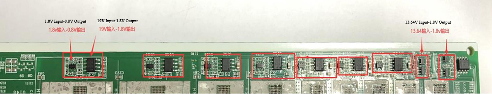
The hash board is composed of 120 BM1489 chips, which are divided into 24 domains, and each domain is composed of 5 ASIC chips; the working voltage of the BM1489 chips used by the L7 hash board is 0.6V; The 24th, 23rd, 22nd, 21st groups (4 groups in total) are powered by the 19.6V output from the boost circuit U13 to the LDO (U249 U247 U243 U239), so that the LDOs of these 4 domains output 1.8V and 0.8V. The power supply of the 20th group LDO is powered by VDD 14.4V to the 20th domain LDO, so that it outputs 1.8V and 0.8V, and the domain voltage is reduced by 0.6V each domain back. As shown in figure:
https://www.zeusbtc.com/share/antminer-l7-hash-board-repair-guide/l7-hash-board-voltage-domain.jpghttps://www.zeusbtc.com/share/antminer-l7-hash-board-repair-guide/l7-hash-board-voltage-domain-schematic.jpghttps://www.zeusbtc.com/share/antminer-l7-hash-board-repair-guide/l7-hash-board-domain-trend.jpghttps://www.zeusbtc.com/share/antminer-l7-hash-board-repair-guide/l7-hash-board-voltage-domain-trend.jpg2. Boost circuit of L7 hash board:
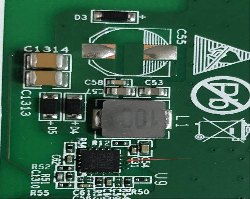
The boost circuit of the L7 hash board is 15V provided by the power supply, and converted to 19.6V, as shown in the figure.
https://www.zeusbtc.com/share/antminer-l7-hash-board-repair-guide/l7-hash-board-boost-circuit.jpghttps://www.zeusbtc.com/share/antminer-l7-hash-board-repair-guide/l7-hash-board-boost-circuit-schematic.jpg3. Signal direction of L7 chip:
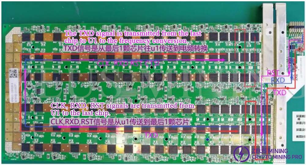
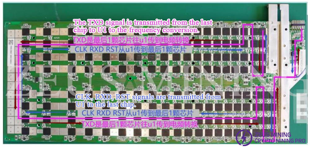
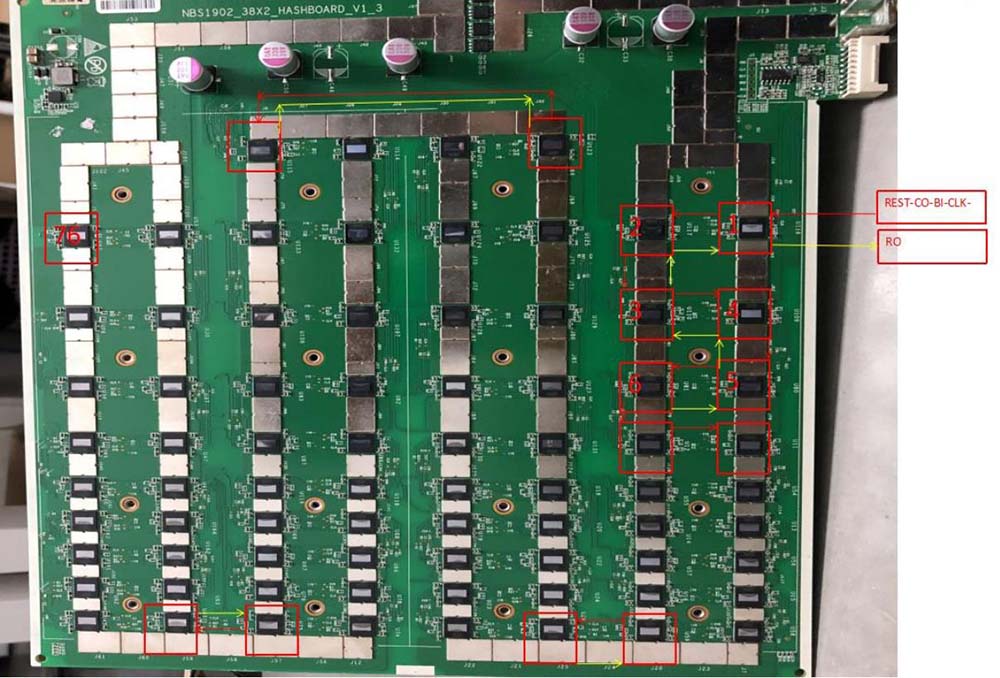
(1) The CLK signal flow direction is generated by Y1&Y2 25M crystal oscillator, Y1 provides chips from No. 01 to No. 60; Y2 provides chips from No. 61 to No. 120, and the voltage measured by the multimeter is about 0.8V-0.9V;
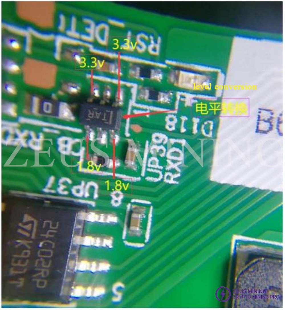
(2) The RST and CI signals flow from the IO port 3 pin (3.3V) into the level conversion IC U1-U3-U4 after conversion, and then from the 01 chip to the 120 chip transmission; when the IO line is not inserted, the voltage is 0V, the voltage during operation is 1.8V;
(3) RX (RI, RO) signal flow direction, from chip No. 120 to chip No. 01, through U1 back to pin 8 of the signal cable terminal and back to the control board; when the IO signal is not inserted, the voltage is 0.3V, and the voltage during operation is 1.8 V;
(4) BO (BI, BO) signal flow, from chip No. 01 to No. 120; the multimeter measures it as 0V;
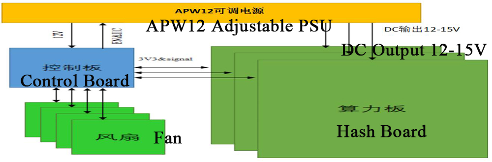
4. The whole Antminer L7 structure:
The whole Antminer L7 is mainly composed of 3 hash boards, 1 control board, APW12 power supply, and 4 cooling fans, as shown in Figure.
https://www.zeusbtc.com/share/antminer-l7-hash-board-repair-guide/l7-miner-architecture.jpgⅤ. Common bad phenomena of the hash board and troubleshooting steps
Phenomenon 1: The single-board test detects that the chip is 0 (PT1/PT2 station)
First step: check the output of the power supply, please check the part of the voltage circled in the picture.
https://www.zeusbtc.com/share/antminer-l7-hash-board-repair-guide/schematic-diagram-of-power-supply-voltage-output.jpgSecond step: check the voltage domain voltage output
The voltage of each voltage domain is about 0.6V, and the 15V power supply generally has the domain voltage. Priority is given to measuring the output of the power supply terminal of the hash board, and whether the MOS is short-circuited (measure the resistor value between pins 1, 4, and 8 ). If 15V is powered but there is no domain voltage, continue to troubleshoot.
https://www.zeusbtc.com/share/antminer-l7-hash-board-repair-guide/mos-tube-voltage-domain.jpgThird step: check the PIC circuit
Measure whether the pin 11 of U6 has output, the voltage is about 3.2V, if there is, please continue to troubleshoot the problem, if there is no 3.2V, please check the connection status of the test fixture cable and the hash board is OK, and re-program the PIC.
https://www.zeusbtc.com/share/antminer-l7-hash-board-repair-guide/pic-circuit-schematic.jpgPIC programming steps:
① Burn the PIC program of the hash board.
Program: 20200101-PIC1704-BM1398-V89.hex
Download the programming tool: PICkit3, pin 1 of the PICkit3 cable corresponds to pin 1 of J3 on the PCB board, and needs to be connected to pins 1, 2, 3, 4, 5, and 6.
https://www.zeusbtc.com/share/antminer-l7-hash-board-repair-guide/pickit3.jpg② Burning software:
(1) Open MPLAB IPE, select device: PIC16F1704, click power to select the power supply mode.
(2) Click operate, select file to find the .HEX file to be burned; click connect, the connection is normal; click the program button, and click "verifiy" after completion, and the verification is completed to prove that the burning is successful.
https://www.zeusbtc.com/share/antminer-l7-hash-board-repair-guide/mplab-ipe-burning-software.jpghttps://www.zeusbtc.com/share/antminer-l7-hash-board-repair-guide/mplab-ipe-running-interface.jpgFourth step: check the boost circuit output
Measure C70 in figure whether the voltage is 23V.
https://www.zeusbtc.com/share/antminer-l7-hash-board-repair-guide/boost-circuit-23v-voltage.jpghttps://www.zeusbtc.com/share/antminer-l7-hash-board-repair-guide/boost-circuit-working-voltage.jpgFifth step: check each group of LDO 1.8V or PLL 0.8V output
https://www.zeusbtc.com/share/antminer-l7-hash-board-repair-guide/ldo-and-pll-test-points.jpghttps://www.zeusbtc.com/share/antminer-l7-hash-board-repair-guide/ldo-and-pll-circuit-schematic.jpgSixth step: check the chip signal output (CLK/CI/RI/BO/RST)
The voltage value range described by the reference signal direction, if the measurement encounters a large deviation of the voltage value, it can be compared with the measurement value of the adjacent group.
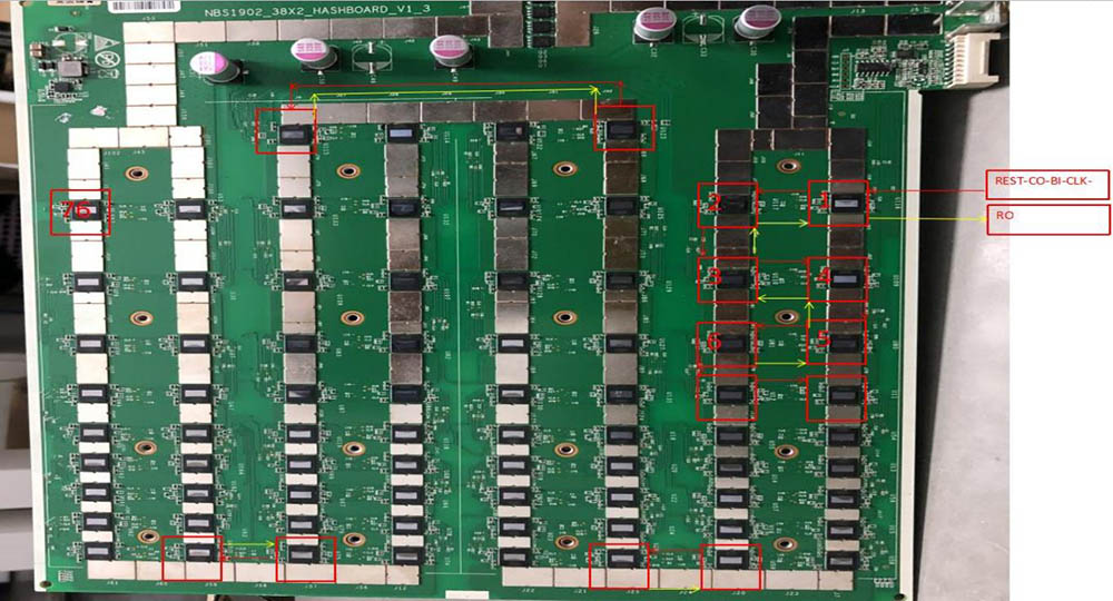
https://www.zeusbtc.com/share/antminer-l7-hash-board-repair-guide/schematic-diagram-of-chip-signal-output.jpgPhenomenon 2: The single-board detection lacks the chip (PT1/PT2 station)
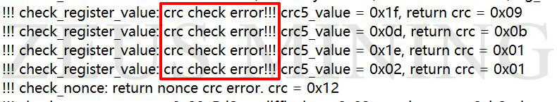
a) LCD screen displays ASIC NG: (0), first measure the total voltage of the domain and the boost circuit 23V is normal, then use a short-circuit probe to short-circuit the RO test point and the 1V8 test point between the 1st and 2nd. Then run the Find Chip program. Looking at the serial port log, if 0 chips are still found at this time, it will be one of the following situations:
a-1) Use a multimeter to measure whether the voltages of the 1V8 and 0V8 test points are 1.8V and 0.8V. If not, it may be that the 1.8V and 0.8V LDO circuits in this domain are abnormal, or two ASIC chips in this domaina are not soldered well, most of them are caused by short circuit of 0.8V and 1.8V chip filter capacitors (measure the resistance value of chip filter capacitors related to the front and back of PCBA)
a-2) Check whether the circuits of U1 and U2 are abnormal, such as resistance soldering, etc.
a-3) Check whether the first chip has pins that are not soldered well (it was found during maintenance, the pins are tin from the side, but they are removed The chip found that the pins were not tinned at all)
b) If one chip can be found in step a), it means that the first chip and the previous circuit are all good. Use the similar method to check the following chips. For example, short-circuit the 1V8 test point and the RO test point between the 38th and 39th chips. If the log can find 38 chips, the first 38 chips are no problem; if 0 chips are still found, check whether the 1V8 is normal first? If it is normal, there is a problem with the chips after 38. Continue to dichotomize until you find the chip in question. Suppose there is a problem with the Nth chip, then when the 1V8 and RO between the N-1th and Nth chips are short-circuited, the N-1 chip can be found. But when 1V8 and RO between the Nth and N+1th chips are short-circuited, not all chips can be found.
c) LCD display X ASIC NG: When a certain chip is fixedly reported, the value of the chip reported in each test usually does not change. In this case, the repair method can be carried out according to the maintenance method of measuring the signal voltage normally.
https://www.zeusbtc.com/share/antminer-l7-hash-board-repair-guide/l7-chip-signal-test-point.jpgPhenomenon 3: Single board Pattern NG, that is, the reply nonce data is incomplete (PT2 station)
Pattern NG is caused by the large difference between the characteristics of the chip and other chips, so just replace the chip. According to the screen prompt of the test fixture or the log information, the replacement rule is: if the appearance of the chip is not damaged, replace the chip with the lowest reply rate in each domain.
The following picture shows one of the test logs. It can be seen from the fixture display that the reply rate of the four chips of asic[10][41][69][75] is low. 69 and 70 are in the same domain, so replace the one with the lowest nonce in 69 and 70. Replace the 10 and 41 at the same time.
PS: need to pay special attention, the number of domain and asic starts from 0, note that the abnormal voltage of the domain will also cause insufficient response of the chip nonce.
https://www.zeusbtc.com/share/antminer-l7-hash-board-repair-guide/test-failed-showing-chip-page.jpgPhenomenon 4: No chip is broken, but the reply rate is not up to standard, and the fixture screen displays P:NG.
P: NG is because some of the chips have a poor reply. You can check the log to replace the 2 with the lowest reply, so that the overall reply rate can reach the standard.
https://www.zeusbtc.com/share/antminer-l7-hash-board-repair-guide/no-chip-display-page.jpghttps://www.zeusbtc.com/share/antminer-l7-hash-board-repair-guide/domain-voltage-is-low.jpgNote: Abnormal domain voltage will also cause insufficient response of chip nonce.
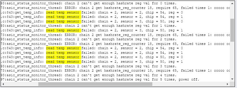
Phenomenon 5: Sensor NG
https://www.zeusbtc.com/share/antminer-l7-hash-board-repair-guide/test-fixture-sensor-ng-page.jpgMaintenance method: When testing PT1 & PT2, look at the serial port print log, confirm that the temperature sensor reports an error, and check the temperature sensor circuit accordingly; first measure whether the power supply of the 8th pin of the temperature sensor is 3.3V, and then check whether the SDA and SCL buses are abnormal.
Requirements for the PT2 test environment: The temperature of the PT2 test environment should be between 25℃ and 30℃. When the ambient temperature is below 25℃, the software will stop the test.
PT2 test power supply requirements: When the PT2 test fixture power supply is under a load of 1500 watts (in the case of testing a board), the actual output voltage cannot be lower than the 0.03V set in the configuration file. (For example, the configuration file requires an output of 13.8V, then the output voltage of the power supply cannot be lower than 13.77V when it is loaded with 1500 watts)
Ⅵ. Control board problems cause the following problems
1. The whole miner does not work
1) Check whether the voltage of several voltage output points is normal, 3.3V short circuit can disconnect U8 first, if it is still short circuit, unplug the CPU and measure. For other abnormal voltages, generally replace the corresponding converter IC.
2) If the voltage is normal, please check the welding condition of the DDR/CPU (X-RAY check on the production side)
3) Try to update the flash program with SD card;
If the miner with the control board card swiping needs to start normally, the following steps are required:
a) After the card is swiped successfully, the green LED indicator is always on, and the power is turned off and restarted;
b) Wait for 30s after powering on again (time course of opening OTP)
c) OTP (One Time Programable) is a memory type of MCU, which means one-time programmable: after the program is burned into the IC, it cannot be changed or cleared again;
Precautions:
(1) Sudden power failure during the OTP opening process or the time is less than 30s will cause the control board to fail to open the OTP function, the control board will not start (not connected to the Internet), and the U1 (control board main control IC FBGA) needs to be replaced. U1 can no longer be used on 19 series;
(2) U1 cannot be used on other series of models if the control board with OTP function is turned on;
https://www.zeusbtc.com/share/antminer-l7-hash-board-repair-guide/l7-control-board.jpg2. The whole miner cannot find the IP
There is a high probability that the IP cannot be found due to abnormal operation. Refer to point 1 for troubleshooting.
Check the appearance and welding condition of the network port, network transformer T1, and CPU.
3. The whole miner cannot be upgraded
Check the appearance and welding condition of the network port, network transformer T1, and CPU.
4. The whole miner fails to read the hash board or the chain is missing
A. Check the cable connection.
B. Check the parts of the control board corresponding to the chain.
C. Check the wave soldering quality of the header pins and the resistance around the plug-in interface.
https://www.zeusbtc.com/share/antminer-l7-hash-board-repair-guide/plugin-interface.jpgⅦ. The whole miner failure phenomenon
1. Preliminary test of the whole machine
Referring to the test process document, the general problems are assembly process problems and control board process problems.
Common phenomenon: IP cannot be detected, abnormal number of fans detected, abnormal detected chain. If there is an abnormality during the test, it should be repaired according to the monitoring interface and the test LOG prompts. The maintenance methods of the initial test and the aging test of the whole machine are the same.
https://www.zeusbtc.com/share/antminer-l7-hash-board-repair-guide/test-results-page.jpg2. Aging test: the old test should be repaired according to the monitored interface test, such as;
1) The fan display is abnormal - we have to check whether the fan works normally, whether the connection with the control board is normal, and whether the control board is abnormal.
2) Less chain: Less chain means that 3 boards are missing 1 board. In most cases, there is a problem with the connection between the hash board and the control board. Check the cable to see if there is an open circuit. If the connection is OK, you can test the board to PT2 to see if it can be tested. If it can be tested, it can basically be determined that it is the control board. If the test fails, use the repair method of PT2 maintenance.
3) Abnormal temperature: Generally, the temperature is high. The maximum PCB temperature set by our monitoring system cannot exceed 90 ℃.
The fan will alarm and it will not work normally. Generally, the ambient temperature is too high, and the abnormal operation of the fan will also cause abnormal temperature.
4) Can not find all the chips (the same can be turned on, but the computing power is 2/3 or 1/3 of the normal value) The number of chips is not enough: If the number of chips is not enough, you can refer to PT2 for testing and repair.
https://www.zeusbtc.com/share/antminer-l7-hash-board-repair-guide/detect-0-chips.jpg5) After running for a period of time, there is no hashrate, and the connection of the mining pool is interrupted, check the network;
https://www.zeusbtc.com/share/antminer-l7-hash-board-repair-guide/network-connection-lost.jpg6) The aging test state of the normal good miner;
https://www.zeusbtc.com/share/antminer-l7-hash-board-repair-guide/l7-miner-aging-test-status.jpgVIII. Other Precautions
Maintenance flow chart
https://www.zeusbtc.com/share/antminer-l7-hash-board-repair-guide/l7-miner-maintenance-flow-chart.jpg1. Routine testing: First, visually inspect the hash board to be repaired to observe whether there is any PCB deformation or scorching. If there is, it must be dealt with first; Whether any parts have obvious burn marks, parts impact offset or missing parts, etc.; Secondly, after the visual inspection is no problem, you can first detect the impedance of each voltage domain, whether there is a short circuit or an open circuit. If found, it must be dealt with in advance. Then, check whether the voltage of each domain is about 0.6V.
2. After the routine inspection is OK (generally the short-circuit inspection of the routine inspection is necessary to avoid burning the chip or other materials due to short-circuit when the power is turned on), the chip can be inspected with a test fixture, and the positioning is determined according to the test results of the test fixture.
3. According to the display results detected by the test fixture, starting from the vicinity of the faulty chip, check the chip test points (CI/NRST/RO/XIN/BI), and the voltages of VDD 0V8 and VDD 1V8.
4. Then according to the signal flow, except for the reverse transmission of the RX signal (chips 120 to 1), the other signals CLK, CI, BI, and RST are transmitted in the forward direction (chips 1 to 120). Through the power supply sequence, find unusual points of failure.
5. When the faulty chip is located, the chip needs to be re-soldered. The method is to add flux (preferably no-clean flux) around the chip, heat the solder joints of the chip pins to a dissolved state, and promote the chip pins and pads to re-grind and collect tin. In order to achieve the effect of re-tinning. If the fault is still the same after re-soldering, the chip can be replaced directly.
6. After repairing the hash board, when using the test fixture to test, it must pass more than two times to be judged as normal. After the replacement parts are completed, wait for the hash board to cool down. After using the test fixture for the first time to test the pass, put it aside before cooling. Wait a few minutes for the hash board to cool completely before doing the second test.
7. After the hash board is repaired OK. Relevant maintenance/analysis records need to be made (requirements for maintenance reports: date, SN, PCB version, tag number, cause of failure, attribution of responsibility for failure, etc.). In order to feedback back to production, after-sales, and research and development.
8. After the document recording is completed, it is then assembled into a complete machine for routine aging.
9. The good products repaired on the production side should be streamlined from the first station of production (at least the appearance inspection and the PT1/PT2 test station)!
10. The repaired defective hash board, the thermal conductive gel must be removed, and the large heat sink should be repainted before it can be streamlined!


 . If there is a 14V power supply, there will generally be a domain voltage output. Under normal circumstances, the voltage is unstable, and the lightning surge will damage the MOS.